

The HT97220(L) is a differential input Direct Drive line driver/headphone amplifier, which can also drive single-ended input signal. It is capable of being driven with 125mW into 32Ω with a 5V supply. The IC is offered with an externally set gain through external resistors (or an internally fixed 6dB gain which needs to be pre-booked. The external gain setting nodes can also be used to configure filters for set-top box applications. The IC has exceptional THD+N over the full audio bandwidth.
Two versions of the IC can be chosen with different turn-on times (tON). The versions for headphone applications feature a tON of 4.2ms while the version, intended for set-top-box applications, which needs to be pre-booked, feature a 130ms tON. An on-chip charge pump inverts the power-supply input, creating a negative rail. The output stage of the amplifier is powered between the positive input supply and the output of the charge pump. The bipolar supplies bias the output about ground, eliminating the need for large, distortion-introducing output coupling capacitors. The IC shutdowns and startups without click-pop noise.
The IC is available in a 3mm x 3mm, 16-pin QFN-PP and is specified over the extended -40°C to +85°C temperature range.
FEATURES
| APPLICATIONS
|
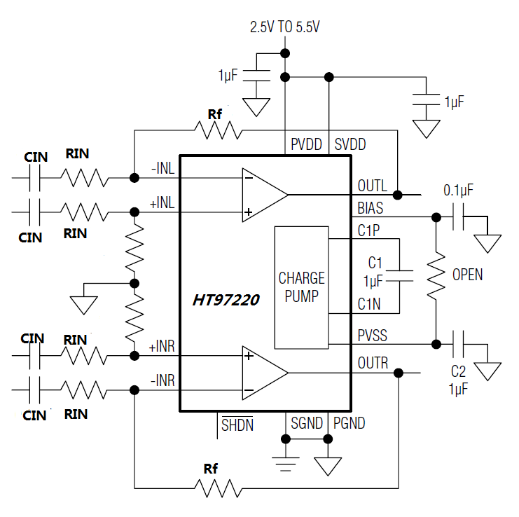

TERMINAL FUNCTION
PIN | NAME | Description |
1 | PVDD | Charge-Pump Power-Supply Input. Bypass to PGND with 1μF. |
2 | C1P | Positive Flying Capacitor Connection. Connect a 1μF capacitor between C1P and C1N. |
3 | PGND | Power Ground. Connect PGND and SGND together at the system ground plane. |
4 | C1N | Negative Flying Capacitor Connection. Connect a 1μF capacitor between C1P and C1N. |
5 | PVSS | Negative Charge-Pump Output. Bypass to PGND with 1μF. |
6 | SGND | Signal Ground. Connect PGND and SGND together at the system ground plane. |
7 | INR+ | Right Positive Polarity Input |
8 | INR- | Right Negative Polarity Input |
9 | SVDD2 | Signal Path Power-Supply Input. Bypass to PGND with 1μF. Connect directly to PVDD. |
10 | OUTR | Right Direct Drive Output |
11 | BIAS | Internal Supply Node. Bypass to PGND with 0.1μF. |
12 | OUTL | Left Direct Drive Output |
13 | SVDD | Signal Path Power-Supply Input. Bypass to PGND with 1μF. Connect directly to PVDD. |
14 | INL- | Left Negative Polarity Input |
15 | INL+ | Left Positive Polarity Input |
16 | nSHDN | Active-Low Shutdown. Drive nSHDN high for normal operation. |
— | EP | Exposed Pad. Electrically connect to PGND or leave unconnected. |