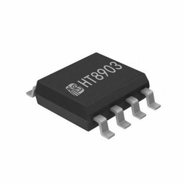
The HT8903 is a non-synchronous boost converter integrated with a 60mΩ power switch to provide a high efficiency and small size solution in portable systems.
The HT8903 has an input voltage range from 2.5 V to 9V to support applications with single cell and two cell Lithium batteries. The device has 7A switch current capability and can provide an output voltage up to 9V.
A function of adjustable Current limitation is available to protect HT8903 from over current during operation, and to prevent the battery from being over-pulled caused by an overload.
The HT8903 is available in SOP8L-PP, with very limited external components, so that it provides space-saving PCB for various applications.
The HT8903 provides 10V output overvoltage protection, and thermal shutdown protection.
FEATURES
| APPLICATIONS
|


TERMINAL FUNCTION
Terminal No. | Name | I/O | Description |
1 | ILIM | O | Adjustable switch peak current limit. An external resister paralleled with a 100pF capacitor should be connected between this pin and the GND pin. |
2,3 | SW | P | The switching node pin of the converter. |
4 | VIN | I | IC power supply input. |
5 | EN | I | Enable logic input. Logic high level enables the device. Logic low level disables the device. |
6 | EAOUT | O | Error amplifier output. Connect a 3.3nF capacity paralleled with 15k resistor to GND. |
7 | FB | I | Regulator Feedback Input. |
8 | VOUT | I | Boost Converter voltage detect pin. |
9 | GND | G | Power ground. Also provides thermal connection from the device to the board. A matching ground pad should be provided on the PCB and the device connected to it via solder. |

